- 您现在的位置:买卖IC网 > Sheet目录345 > MT42L256M32D4KP-3 IT:A (Micron Technology Inc)IC LPDDR2 SDRAM 8GBIT 168FBGA
�� �
�
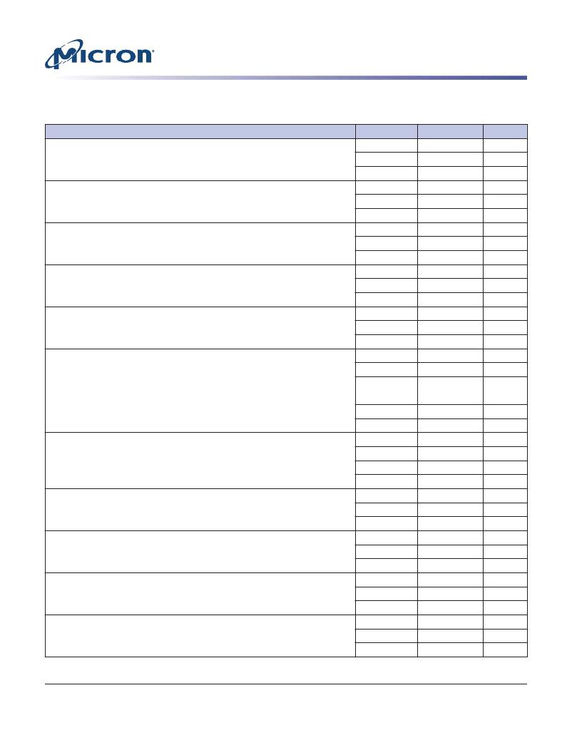
�2Gb:� x16,� x32� Mobile� LPDDR2� SDRAM� S4�
�Electrical� Specifications� –� I� DD� Specifications� and� Conditions�
�Table� 59:� I� DD� Specification� Parameters� and� Operating� Conditions� (Continued)�
�Notes� 1–3� apply� to� all� parameters� and� conditions�
�Parameter/Condition�
�Idle� power-down� standby� current� with� clock� stop:� CK� =� LOW,� CK#� =�
�HIGH;� CKE� is� LOW;� CS#� is� HIGH;� All� banks� are� idle;� CA� bus� inputs� are� stable;�
�Data� bus� inputs� are� stable�
�Idle� non-power-down� standby� current:� t� CK� =� t� CKmin;� CKE� is� HIGH;� CS#� is�
�HIGH;� All� banks� are� idle;� CA� bus� inputs� are� switching;� Data� bus� inputs� are� sta-�
�ble�
�Idle� non-power-down� standby� current� with� clock� stopped:� CK� =� LOW;�
�CK#� =� HIGH;� CKE� is� HIGH;� CS#� is� HIGH;� All� banks� are� idle;� CA� bus� inputs� are�
�stable;� Data� bus� inputs� are� stable�
�Symbol�
�I� DD2PS1�
�I� DD2PS2�
�I� DD2PS,in�
�I� DD2N1�
�I� DD2N2�
�I� DD2N,in�
�I� DD2NS1�
�I� DD2NS2�
�I� DD2NS,in�
�Power Supply�
�V� DD1�
�V� DD2�
�V� DDCA� ,� V� DDQ�
�V� DD1�
�V� DD2�
�V� DDCA� ,� V� DDQ�
�V� DD1�
�V� DD2�
�V� DDCA� ,� V� DDQ�
�Notes�
�4�
�4�
�4�
�Active� power-down� standby� current:�
�t� CK�
�=�
�t� CKmin;�
�CKE� is� LOW;� CS#� is�
�I� DD3P1�
�V� DD1�
�HIGH;� One� bank� is� active;� CA� bus� inputs� are� switching;� Data� bus� inputs� are�
�stable�
�Active� power-down� standby� current� with� clock� stop:� CK� =� LOW,� CK#� =�
�HIGH;� CKE� is� LOW;� CS#� is� HIGH;� One� bank� is� active;� CA� bus� inputs� are� stable;�
�Data� bus� inputs� are� stable�
�Active� non-power-down� standby� current:� t� CK� =� t� CKmin;� CKE� is� HIGH;� CS#�
�is� HIGH;� One� bank� is� active;� CA� bus� inputs� are� switching;� Data� bus� inputs� are�
�stable�
�Active� non-power-down� standby� current� with� clock� stopped:� CK� =�
�LOW,� CK#� =� HIGH� CKE� is� HIGH;� CS#� is� HIGH;� One� bank� is� active;� CA� bus� inputs�
�are� stable;� Data� bus� inputs� are� stable�
�I� DD3P2�
�I� DD3P,in�
�I� DD3PS1�
�I� DD3PS2�
�I� DD3PS,in�
�I� DD3N1�
�I� DD3N2�
�I� DD3N,in�
�I� DD3NS1�
�I� DD3NS2�
�I� DD3NS,in�
�V� DD2�
�V� DDCA� ,� V� DDQ�
�V� DD1�
�V� DD2�
�V� DDCA� ,� V� DDQ�
�V� DD1�
�V� DD2�
�V� DDCA� ,� V� DDQ�
�V� DD1�
�V� DD2�
�V� DDCA� ,� V� DDQ�
�4�
�4�
�4�
�4�
�Operating� burst� READ� current:�
�t� CK�
�=�
�t� CKmin;�
�CS#� is� HIGH� between� valid�
�I� DD4R1�
�V� DD1�
�commands;� One� bank� is� active;� BL� =� 4;� RL� =� RL� (MIN);� CA� bus� inputs� are�
�switching;� 50%� data� change� each� burst� transfer�
�I� DD4R2�
�I� DD4R,in�
�V� DD2�
�V� DDCA�
�I� DD4RQ�
�V� DDQ�
�5�
�Operating� burst� WRITE� current:�
�t� CK�
�=�
�t� CKmin;�
�CS#� is� HIGH� between� valid�
�I� DD4W1�
�V� DD1�
�commands;� One� bank� is� active;� BL� =� 4;� WL� =� WLmin;� CA� bus� inputs� are� switch-�
�ing;� 50%� data� change� each� burst� transfer�
�I� DD4W2�
�I� DD4W,in�
�V� DD2�
�V� DDCA� ,� V� DDQ�
�4�
�All-bank� REFRESH� burst� current:�
�t� CK�
�=�
�t� CKmin;�
�CKE� is� HIGH� between� valid�
�I� DD51�
�V� DD1�
�commands;� t� RC� =� t� RFCabmin;� Burst� refresh;� CA� bus� inputs� are� switching;� Data�
�bus� inputs� are� stable�
�All-bank� REFRESH� average� current:� t� CK� =� t� CKmin;� CKE� is� HIGH� between�
�valid� commands;� t� RC� =� t� REFI;� CA� bus� inputs� are� switching;� Data� bus� inputs� are�
�stable�
�I� DD52�
�I� DD5IN�
�I� DD5AB1�
�I� DD5AB2�
�I� DD5AB,in�
�V� DD2�
�V� DDCA� ,� V� DDQ�
�V� DD1�
�V� DD2�
�V� DDCA� ,� V� DDQ�
�4�
�4�
�Per-bank� REFRESH� average� current:�
�t� CK�
�=�
�t� CKmin;�
�CKE� is� HIGH� between�
�I� DD5PB1�
�V� DD1�
�6�
�valid� commands;� t� RC� =� t� REFI/8;� CA� bus� inputs� are� switching;� Data� bus� inputs�
�are� stable�
�I� DD5PB2�
�I� DD5PB,in�
�V� DD2�
�V� DDCA� ,� V� DDQ�
�6�
�4,� 6�
�PDF:� 09005aef83f3f2eb�
�2gb_mobile_lpddr2_s4_g69a.pdf� –� Rev.� N� 3/12� EN�
�116�
�Micron� Technology,� Inc.� reserves� the� right� to� change� products� or� specifications� without� notice.�
�2010� Micron� Technology,� Inc.� All� rights� reserved.�
�发布紧急采购,3分钟左右您将得到回复。
相关PDF资料
MT45W1MW16BDGB-708 AT
IC PSRAM 16MBIT 104MHZ 54VFBGA
MT48H32M16LFB4-75B IT:C
IC SDRAM 512MB 54VFBGA
MT48H8M16LFB4-75 IT:K TR
IC SDRAM 128MBIT 133MHZ 54VFBGA
MTC100-JA2-P34
CONTACT INSERT PIN
MX841BE
IC CONVERTER WHITE LED 8-SOIC
MXHV9910BTR
IC LED DRIVER HIGH BRIGHT 8-SOIC
MXN12FB12F
MOTOR BRUSHED DC 12V 2922RPM
MXN13FB08B1
MOTOR BRUSHED DC 8V 4714RPM
相关代理商/技术参数
MT42L256M32D4KP-MS
制造商:Micron Technology Inc 功能描述:256MX32 LPDDR2 PLASTIC IND TEMP GREEN WFBGA 1.2V - Bulk